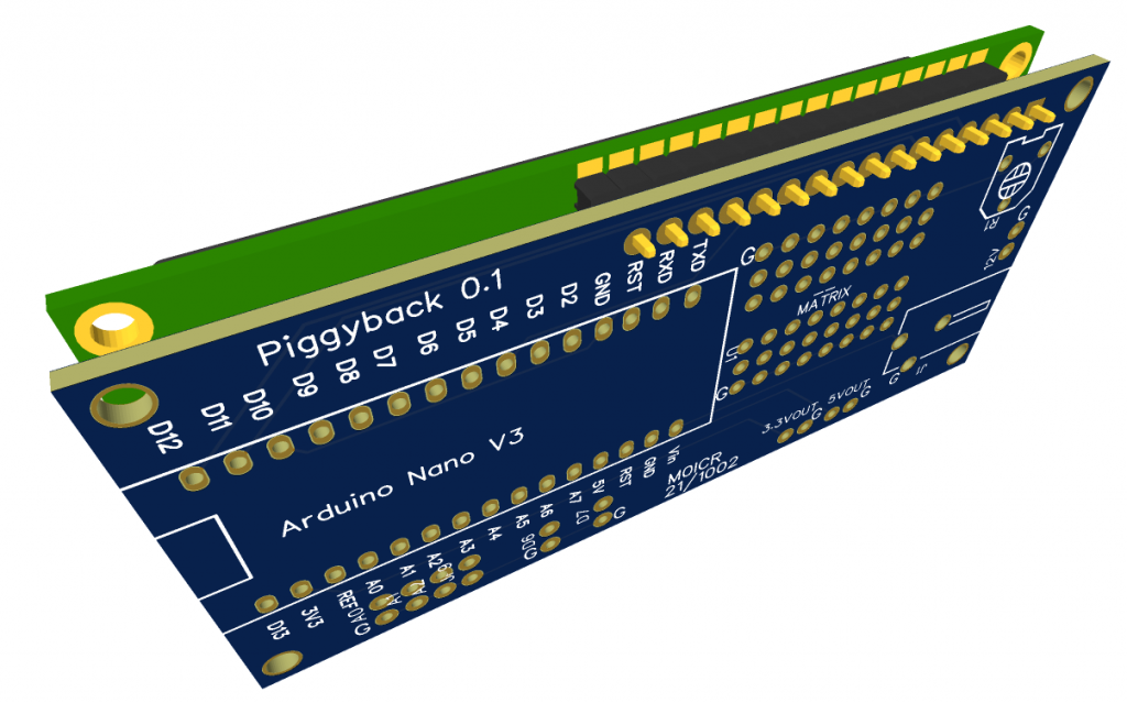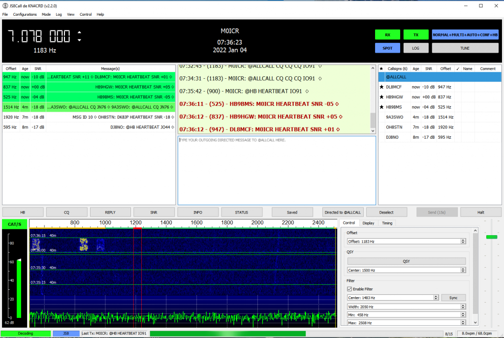
Learning to use EasyEDA and designing a PCB that I am calling the piggyback.
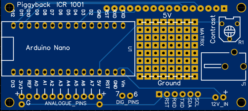
A Hitachi 44780 LCD module (1602 or 2004) will be mounted in front of he board (the 16 pins at the top), I2C connection(s) will also be possible. The Arduino Nano (U1) is mounted on the left of the board with breakout fins for each of the pins (I am not entirely happy with the design yet as, on reflection) I really want to add the possibility of breaking out ALL of the Nano pins (including the digital ones not yet connected). Finally there is a matrix board for prototyping on the right of the board and also a contrast preset (R1) (for the 44780) and a DC connector jack (J1).
Here is an idea of what it looks like in 3D with the 44780 fitted (the PCB was an earlier iteration).